


You can understand the meaning, types, and applications of perovskites, as well as how to choose materials, fabricate, and optimize perovskite-based devices in this comprehensive guide for beginners.
Overview
Perovskites are a class of materials with the same crystal structure as the mineral calcium titanate (CaTiO₃). They have a general chemical formula of ABX₃, where A and B are cations of different sizes, and X is an anion that bonds to both.
Perovskites have attracted significant attention in fields like photovoltaics, optoelectronics, LEDs, and photocatalysis due to their excellent light absorption, tunable bandgap, and high carrier mobility.
Understanding perovskites is essential for researchers and engineers who want to develop high-efficiency solar cells, advanced photodetectors, or next-generation optoelectronic devices.
Perovskite Types
Organic–Inorganic Hybrid Perovskites
These perovskites combine organic cations (like methylammonium, MA⁺) with inorganic frameworks (like PbI₆ octahedra). They are the most widely used in solar cell research due to high power conversion efficiency.
All-Inorganic Perovskites
All-inorganic perovskites, such as CsPbI₃ or CsPbBr₃, replace organic cations with inorganic ones, offering better thermal stability and longer device lifetimes, suitable for harsh environmental conditions.
Double Perovskites
Double perovskites have two different B-site cations (A₂BB’X₆), which reduce toxicity (e.g., replacing lead with tin or bismuth) while maintaining desirable optoelectronic properties.
Two-Dimensional (2D) Perovskites
2D perovskites have layered structures, providing higher stability against moisture and heat. They are especially useful in tandem solar cells and flexible optoelectronic devices.
Types of Perovskite Devices
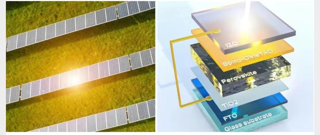
Perovskite Solar Cells (PSCs)
• Convert sunlight into electricity with high efficiency, reaching over 25% in laboratory settings.
• Can be fabricated on rigid or flexible substrates, suitable for building-integrated photovoltaics (BIPV).
Perovskite LEDs (PeLEDs)
• Emit light efficiently across visible and near-infrared wavelengths.
• Used in displays, lighting, and optical communication.
Perovskite Photodetectors
• High sensitivity and fast response speed for imaging and sensing applications.
• Tunable wavelength response depending on the perovskite composition.
Perovskite Photocatalysts
• Enable solar-driven chemical reactions such as water splitting and CO₂ reduction.
• Offer a promising approach for sustainable energy solutions.
What Should I Consider When Working with Perovskites?
• Which type of perovskite suits your application? Hybrid, inorganic, 2D, or double perovskite?
• Stability: How resistant is the material to moisture, heat, and light degradation?
• Fabrication method: Spin coating, vapor deposition, or blade coating?
• Bandgap tuning: Can the perovskite composition be adjusted for optimal absorption or emission?
• Toxicity: Does it contain lead, and what safety measures are needed?
• Device architecture: Which structure maximizes efficiency? Planar, mesoporous, or tandem?
• Encapsulation: How will you protect the perovskite layer from environmental factors?
Best Perovskite Materials You Can Work With in 2025
#1 MAPbI₃ (Methylammonium Lead Iodide)
• Popular in lab-scale solar cells for its high efficiency and ease of processing.
• Best suited for researchers exploring fundamental perovskite optoelectronic properties.
#2 CsPbBr₃ (Cesium Lead Bromide)
• Offers excellent thermal stability and is ideal for LEDs and photodetectors.
• Used in devices that require long operational lifetimes under heat.
#3 FA₀.₈MA₀.₂PbI₃ (Formamidinium-Methylammonium Mixed Perovskite)
• Combines stability with high efficiency in perovskite solar cells.
• Increasingly used in commercial PSC development.
How to Work with Perovskite Materials?
Mastering perovskite fabrication and device integration requires careful handling and practice. Here are 10 beginner-friendly steps:
- Ensure your laboratory environment is clean and humidity-controlled.
- Prepare high-purity precursors and solvents.
- Mix the perovskite precursor solution accurately according to the desired stoichiometry.
- Filter the solution to remove any particulate matter.
- Choose the appropriate substrate (glass, ITO, or flexible substrate) and clean it thoroughly.
- Deposit the perovskite layer using spin coating, blade coating, or vapor deposition.
- Anneal the perovskite layer under controlled temperature to form a uniform crystal structure.
- Add charge transport layers (electron and hole transport) as required.
- Encapsulate the device to protect against moisture and oxygen.
- Test the device performance and iterate process parameters for optimization.
Conclusion
Perovskites are revolutionizing photovoltaics and optoelectronics with their high efficiency, tunable properties, and versatile applications. By understanding the types, device architectures, and fabrication methods, you can confidently begin experimenting with perovskites and transition from a novice to an experienced researcher in this exciting field.